With PiCtory, you can configure your RevPi AIO. In this chapter, we will describe the settings of the Value Editors for analogue outputs in greater detail.
Requirements:
- A web browser is installed on your PC (e.g. Chrome or Firefox).
- RevPi Connect is to be found in your network.
Let’s go!
Your AIO has 2 analog outputs. The outputs can emit either voltage or current. You can connect up actuators like for example frequency converters for speed control.
In order for configuration to function, it is important that your devices are connected to the right output pins.
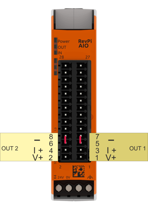
| Output 1 | |
| PIN | Use |
| 1 | V+ positive output for voltage ranges channel 1 |
| 3 | I+ positive output for current ranges channel 1 |
| 5 | common ground for both output channels 1 and 2 (current and voltage) |
| 7 | common ground for both output channels 1 and 2 (current and voltage) |
| Output 2 | |
| PIN | Use |
| 2 | V+ positive output for voltage ranges channel 2 |
| 4 | I+ positive output for current ranges channel 2 |
| 6 | common ground for both output channels 1 and 2 (current and voltage) |
| 8 | common ground for both output channels 1 and 2 (current and voltage) |
Please remember that you can always only display current or voltage on one channel even though there are two separate connections.
- Open your web browser.
- Enter the IP address of your RevPi Connect in the address bar of your web browser.
The login window appears.
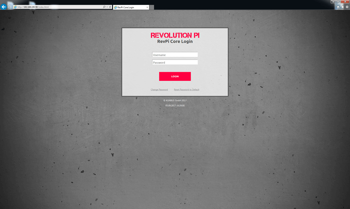
- Log in with the username “admin”.
- Enter the password. You can find it on the sticker on the side of your RevPi Connect.
- Click on “Login”
You will now see the current device status of your RevPi Connect.

- Click the “Apps” tab.
- Click the start button behind the entry “PiCtory”.
PiCtory opens.
- Open the folder “I/O Devices” in the device catalog.
- Select AIO.
- Drag and drop the AIO in the empty slot on the Configuration Board.
- Determine the basic settings for your adapter in the “Device Data” section. This is optional. The settings can however be useful when using many devices and you would like to process the data in another programme at a later point in time.
You can configure your outputs in Value Editor. The detailed settings are to be found in the following table.
| PiCtory setting | Value | Function |
| Output1 Range, Output2Range |
|
Set here the value ranges for the current or voltage that the outputs should emit. |
| Output1EnableSlew, Output2EnableSlew |
On = use slew rate Off= don’t use slew rate |
Here you can determine whether you would like to use a slew rate for the respective output. The slew rate controls the rate at which the output voltage or the strength of the output current is changed when you set a new value for an output in the process image. |
| Output1SlewStepSize, Output1SlewStepSize |
|
Here you can select the slew rate step size for the respective function. Step size 1 corresponds to the smallest bit value (LSB) from the converter. Together with the clock frequency, the step size determines the slew rate between two analog values. |
| Output1SlewUpdateFreq, Output1SlewUpdateFreq |
|
Here you can select the step clock frequency for the slew rate of the respective output. Together with the clock frequency, the step size determines the slew rate between two analog value. |
| Scaling output 1: Output1Multiplier Output1Divisor Output1Offset Scaling output 2: Output2Multiplier Output2Divisor Output2Offset |
|
Here you can set a scaling for every output channel. It is determined by the three configuration values and calculated according to the following formula from the original value: (available in mV or µA respectively):
Y = Multiplier/Divisor*X + Offset X is the value for the output, |
Please remember that you can always only display current or voltage on one channel even though there are two separate connections.
The scaling can be used for the conversion into other units or for a subsequent calibration of an actuator. When calculating in an AIO module, a 32-bit Integer Arithmetic is used. The results are then sent again as 16-bit values to DAC. Should the result Y exceed the limits of a 16-bit signed value, then the error is recognised and the value limited. The output values for scaling factor 1 always have to be stored in the process image in the unit mV or µA respectively.
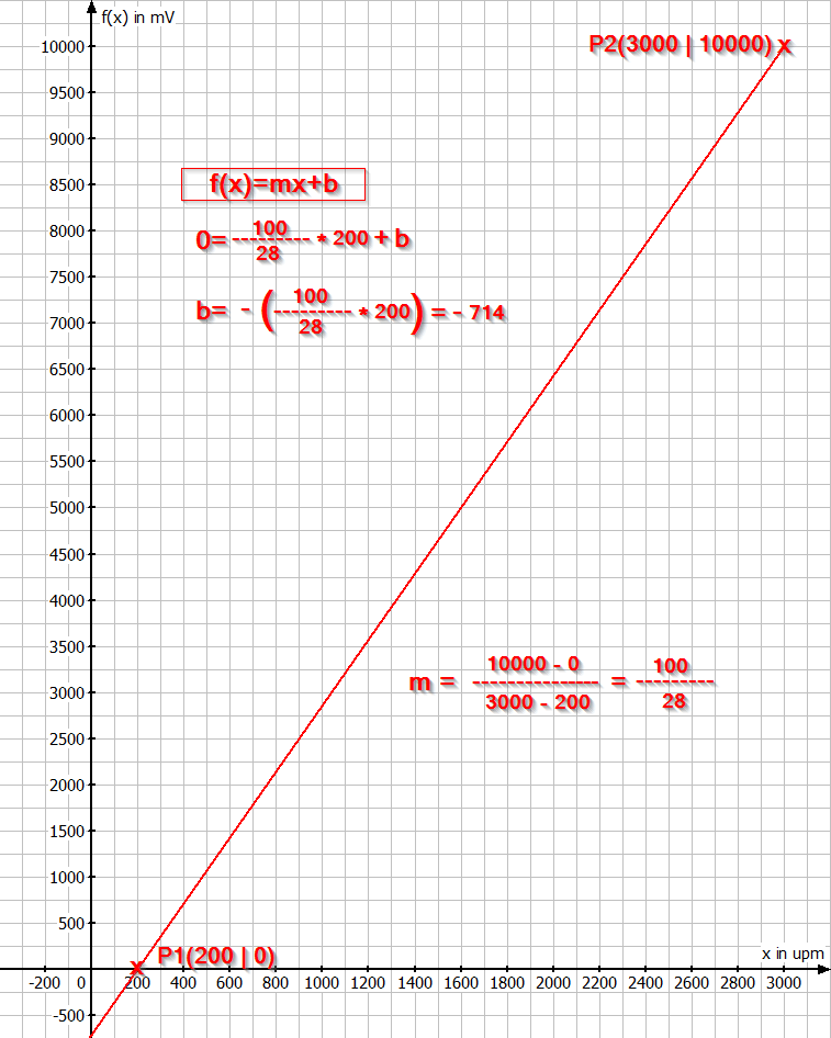
Example:
A frequency converter triggers an electric motor. It has an analog input of 0 to 10 V, whereby 0 V corresponds to a speed of 200 rpm and 10 V a speed of 3000 rpm. To store the speed in rpm in the process image, you have to select the parameters for the output range 0-10 V as follows:
Multiplier = 100, Divisor = 28, Offset = -714
The slew rate settings have the following meaning:
Let’s assume, you have selected an output range of 0 to 10 V. In the process image, there is an output value of 3 V for channel 1. The value should now be changed to 8 V. You therefore should now write the figure 8000 instead of 3000 mV in the respective offset in the process image. In the next PiBridge cycle, the figure is then consigned to the DAC (Digital to Analog Converter) which then generates the analogue voltage for the output. This takes place with a certain delay time of 10-40 ms depending on the load on the PiBridge (which depends on the configuration). After the delay, the output voltage will quickly jump from 3 V to 8 V. The slew rate of the voltage is only dependent on the total capacity at the output (which amongst other things is dependent on the connected devices). As a rule, it should amount to a few µs. The slew rate is often not desired because it has an extremely high frequency ratio that can lead to interference radiation and other problems. You can therefore artificially reduce the slew rate. To do so, click on “Output?EnableSlew”. Now the DAC will, as soon as it has received the new data (8000), increase the output voltage in small steps until 8 V is reached. You should set the amplitude by yourself by going to “Output?SlewStepSize”. This step size will be shown as a “LSB” (Last Significant Bit). As our converter works with a 16-bit resolution in every output range, the step size of the lowest-valued bit (LSB) measures, in the 0-10V range, 10V/2^16 = 0.15 mV (or respectively 0.30 µA in the 4-20 mA range). The number of minute steps that the DAC needs depends therefore only on the voltage jump: In our example, it is, for a step size of 1, therefore 5000 mV / 0.15 mV = 33,333 steps. The time in which these steps are performed is determined by the clock speed by which the steps are integrated into the signal. They can be set by yourselves by means of the “Output?SlewClock” parameter. When the clock speed is set at 3.3 kHz, the edge needs from 5 V, therefore 33,333* 1/3300 s = 10 s. When set at 258 kHz, it is therefore 130 ms. The slew rate is, for a 3.3 kHz clock speed, therefore 0.5 V/s or 38 V/s respectively when the clock speed is 258 kHz. You can obviously significantly increase the slew rate with larger step sizes but the signal will also “skip” so that it will receive significantly greater share of high frequency signals.
- Click on “File>Save”. You thus save your file.
- Click “Tools>Reset Driver”. You thus activate the changes for the adapter.
Should an error occur, you will receive error messages in the input values of the process image with the names OutputStatus_1 und OutputStatus_2. The respective bits in the status bytes have the following meaning:
| Bit position | Status message |
| 0 (LSB) | Temperature error from the output chip. The output chip is overheated as a result of overloading (short circuit). |
| 1 | Open Load Error from current output. In the “Current Output” operating mode, the connected circuit is highly resistive because, for example, the supply has been interrupted. |
| 2 | Internal CRC error from output chip. The error points to a hardware defect or serious external interference signals. |
| 3 | Range error: the output value in the process image is below the configured output range. |
| 4 | Reserved for internal purposes |
| 5 | The supply voltage for the module is less than 10.2 V. The outputs have been shut down. |
| 6 | The supply voltage for the module is more than 28.8 V. The outputs have been shut down. |
| 7 (MSB) | Timeout in the connection to RevPi Connect (e.g. due to a disturbance to the PiBridge or if the PiControl drive program no longer runs properly on the RevPi Connect. The outputs have been shut down. |
Please note: in all the situations in which the outputs have been shut down for safety reasons, the outputs are then only available after the device has been restarted or the PiBridge has been reset (e.g. piTest -x).
- Would you like to continue to use the settings in logiCAD3, Python or C?
- Then click on “File>Export“.
A window will now open. Here you can determine the format of the file and give the file a name.
You can choose between 2 formats:
Export 01 creates a file suitable for use in logiCAD3.
Export 02 creates an Offset List that you can use as basic information for an own C or programme.
- Select a format with which you would like to work.
- Write in a file name
- Click on „Ok“.